

Nvidia Ampere vs. AMD RDNA 2: Battle of the Architectures
For GPU enthusiasts, it'due south been a long wait. Nvidia kept the Turing line going for two years before replacing information technology with Ampere in September 2022. AMD were a picayune kinder, leaving a 15 calendar month gap betwixt their new designs, but about people weren't interested in that.
What they wanted to see was AMD launching a top end model to compete caput-to-head with the all-time from Nvidia. They did merely that and now that we've seen the results, PC gamers are now spoilt for choice (at to the lowest degree theoretically), when it comes to spending their dollars on the best performing graphics cards.
Merely what about the fries powering them? Is one of them fundamentally improve than the other?
Read on to see how Ampere and RDNA two battle it out!
Commodity Index
- Nodes and die sizes
- Overall structure of Ampere GA102 and RDNA 2 Navi 21
- How everything is organized inside the fries
- Counting cores the Nvidia way
- Ray Tracing
- Retentivity system, multi-level caches
- Rendering pipelines, SAM, RTX IO
- Multimedia engine, streaming
- Built for compute, built for gaming
Nvidia shrinks, AMD grows
Nodes and dice sizes
Loftier-end GPUs have been considerably bigger than CPUs for a number of years, and they've been steadily increasing in size. AMD'southward latest offer is roughly 520 mm2 in surface area, more than double the size of their previous Navi chip. It's not their largest, though -- that honor goes to the GPU in their new Instinct MI100 accelerator, at around 750 mmii.
The last time AMD made a gaming processor anywhere most the size of Navi 21 was for the Radeon R9 Fury and Nano cards, which sported the GCN iii.0 architecture in a Fiji chip. It was 596 mmii in die area, but it was manufactured on TSMC's 28HP procedure node.
AMD has been using TSMC's much smaller N7 process since 2022 and the biggest chip from that product line was the Vega 20 (as found in the Radeon VII), with an area of 331 mmii. All of their Navi GPUs are made on a slightly updated version of that process, chosen N7P, so it makes to compare these products.

But when it comes to sheer die size, Nvidia takes the crown, not that this is necessarily a skilful thing. The latest Ampere-based fleck, the GA102, is 628 mm2. That's really almost 17% smaller than its forefather, the TU102 -- that GPU was a staggering 754 mm2 in die expanse.
Both pale in size when compared to Nvidia'due south monstrous GA100 scrap - used in AI & data centers, this GPU is 826 mm2 and it's a TSMC N7 bit. While never designed to power a desktop graphics carte, information technology does show what scale of GPU manufacturing is possible.
Putting them all side-by-side highlights only how beefy Nvidia'southward biggest GPUs are. The Navi 21 looks fairly svelte, although there's more to a processor than just dice expanse. The GA102 is packing effectually 28.3 billion transistors, whereas AMD'southward new chip sports 5% fewer, at 26.8 billion.
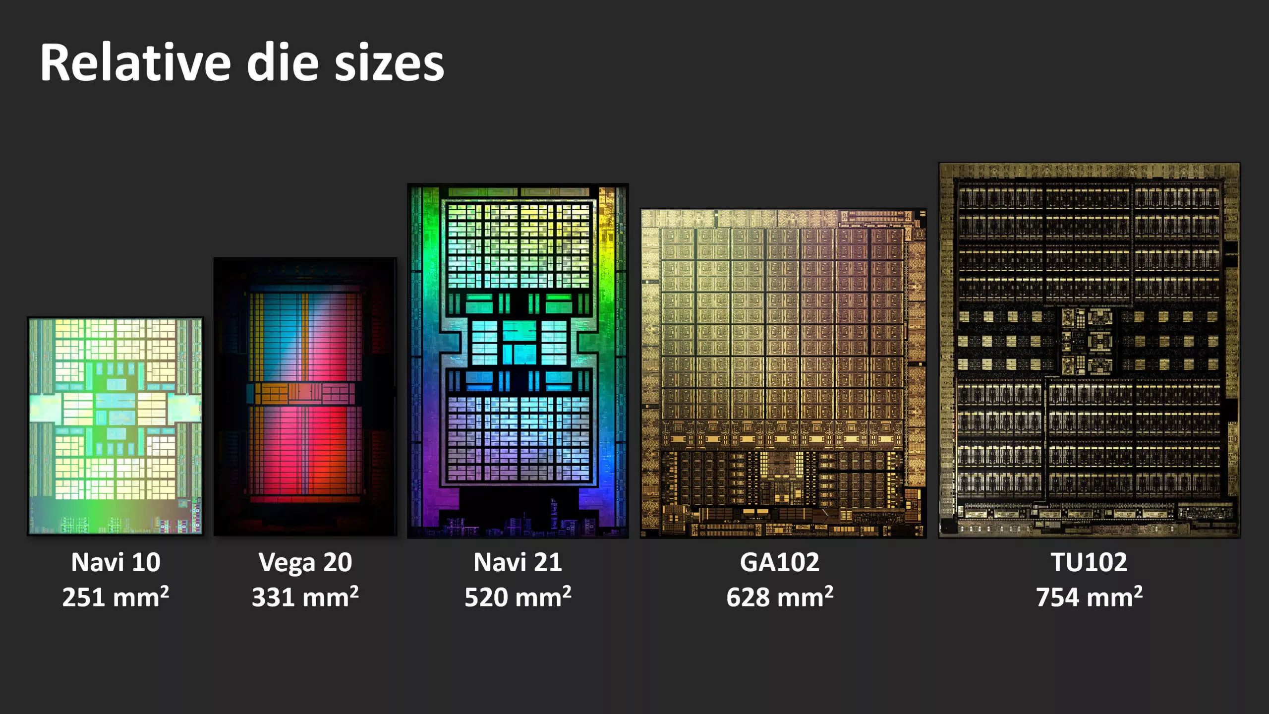
What we don't know is how many layer each GPU is congenital of, and so all we can compare is the ratio of transistors to die area, typically called dice density. The Navi 21 is roughly 51.v million transistors per square mm, but the GA102 is notably lower at 41.1 -- information technology could be that Nvidia's chip is stacked a little higher than AMD's, just it's more than probable to be an indication of process node.
As already mentioned, the Navi 21 is manufactured by TSMC, using their N7P product method, which offers a small increase in performance over N7; just for their new offering, the GA102, Nvidia turned to Samsung for production duties. The Southward Korea semiconductor behemothic is using a tweaked version, specifically for Nvidia, of their so-called 8 nm node (labelled as 8N or 8NN).
These node values, 7 and 8, take lilliputian to do with the actual size of the components with the chips: they're only marketing terms, used to differentiate between the various product techniques. That said, even if the GA102 has more layers than the Navi 21, the die size does take one particular impact.

Microprocessors and other fries are fabricated from large, round discs of highly refined silicon and other materials, called wafers. TSMC and Samsung utilise 300 mm wafers for AMD and Nvidia, and each disc will generate more than chips using smaller dies compared to larger ones.
The difference is unlikely to be huge, just when every wafer costs thousands of dollars to produce, AMD have a small advantage over Nvidia, when it comes to keeping manufacturing costs down. That'due south bold, of grade, Samsung or TSMC aren't doing some kind of fiscal bargain with AMD/Nvidia.
All of this die size and transistor count shenanigans would be for naught, if the chips themselves weren't whatsoever good at what they're design to do. So allow's dig into the layouts of each new GPU and see what's underneath their hoods.
Dissecting the dies
Overall structure of Ampere GA102 and RDNA ii Navi 21
We kickoff our exploration of the architectures with a look at the overall structure of the Ampere GA102 and RDNA two Navi 21 GPUs -- these diagrams don't necessarily show u.s.a. how everything is physically laid out, only they give a clear indication as to how many components the processors have.
In both cases, the layouts are very familiar, as they are essentially expanded versions of their predecessors. Adding more units to process instructions volition always increase the performance of a GPU, because at high resolutions in the latest 3D blockbusters, the rendering workloads involve a huge number of parallel calculations.

Such diagrams are useful, but for this item analysis, it'southward actually more interesting looking at where the diverse components are within the GPU dies themselves. When designing a large calibration processor, you generally want shared resources, such equally controllers and cache in a central position, to ensure every component has the same path to them.
Interface systems, such as local memory controllers or video outputs, should go on the edges of the fleck to brand it easier to connect them to the thousands of individual wires that link the GPU to the rest of the graphics carte du jour.
Below are false-color images of AMD's Navi 21 and Nvidia's GA102 dies. Both have been run through some image processing to make clean upwardly the images, and both are really only showing 1 layer inside the chip; but they do give us a superb view of the innards of a modern GPU.
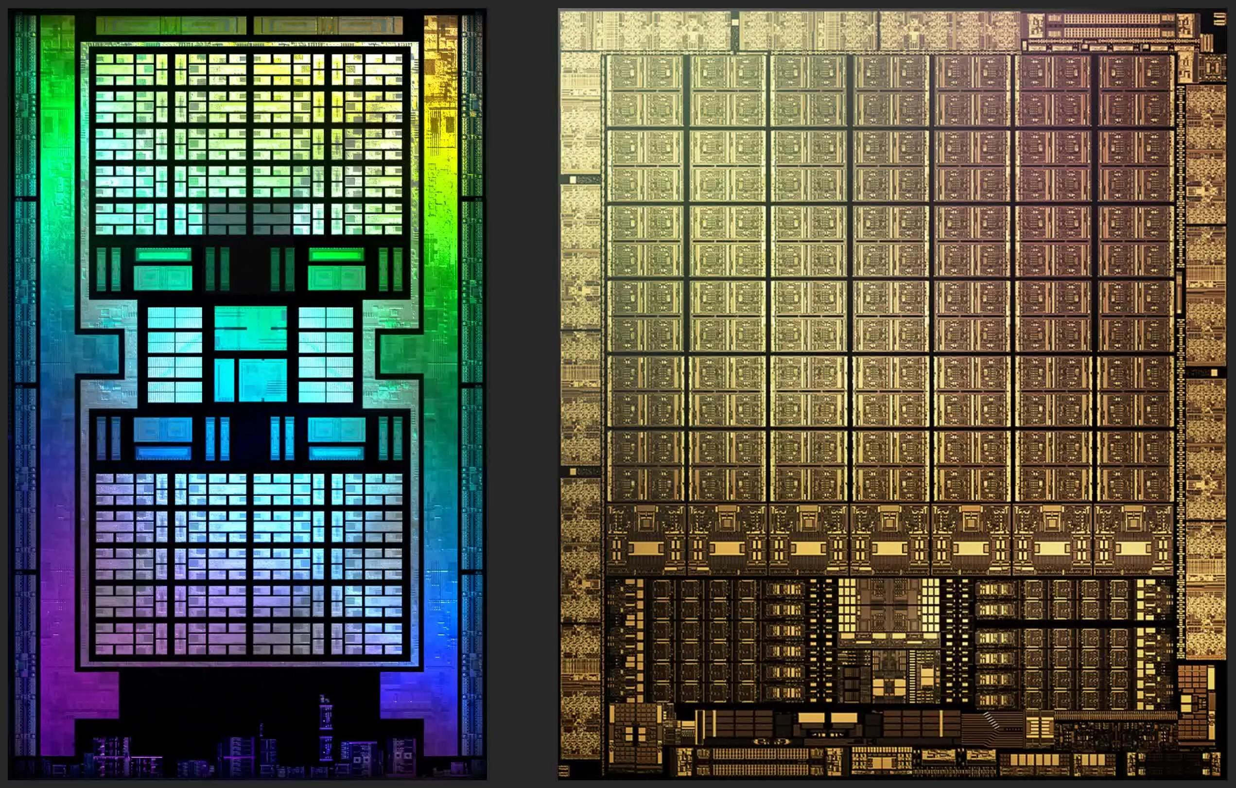
The most obvious deviation between the designs is that Nvidia hasn't followed a centralized arroyo to the chip layout -- all of the system controllers and main cache are at the bottom, with the logic units running in long columns. They've done this in the past, simply only with centre/lower finish models.
For case, the Pascal GP106 (used in the likes of the GeForce GTX 1060) was literally half of a GP104 (from the GeForce GTX 1070). The latter was the larger chip, and had its cache and controllers in the middle; these moved to the side in its sibling, but only because of the design had been split.

For all their previous top end GPU layouts, Nvidia used a archetype centralized organisation. So why the change here? It can't be for interface reasons, every bit the memory controllers and the PCI Express system all run around the edge of the dice.
It won't be for thermal reasons either, because fifty-fifty if the enshroud/controller part of the die ran hotter than the logic sections, y'all'd still desire it in the heart to take more silicon around it to assist absorb and dissipate the rut. Although we're not totally sure of the reason for this alter, we doubtable that it's to do with the changes Nvidia accept implemented with the ROP (render output) units in the fleck.
We'll look at those in more particular afterward, but for now let's only say that while the change in layout looks odd, it won't make a significant difference to performance. This is because 3D rendering is riddled with lots of long latencies, typically due to having to wait for data. And so the additional nanoseconds added by having some logic units further from the cache than others, all get hidden in the yard scheme of things.
Before nosotros motion on, information technology'southward worth remarking on the engineering changes AMD implemented in the Navi 21 layout, compared to the Navi ten that powered the likes of the Radeon RX 5700 XT. Fifty-fifty though the new bit is double the size, both in terms of area and transistor count, than the earlier one, the designers likewise managed to also improve the clock speeds, without significantly increasing power consumption.
For example, the Radeon RX 6800 XT sports a base clock and boost clock of 1825 and 2250 MHz respectively, for a TDP of 300 West; the same metrics for the Radeon RX 5700 XT were 1605 MHz, 1905 MHz, and 225 Due west. Nvidia raised the clock speeds with Ampere, besides, but some of that can be attributed towards using a smaller and more than efficient process node.
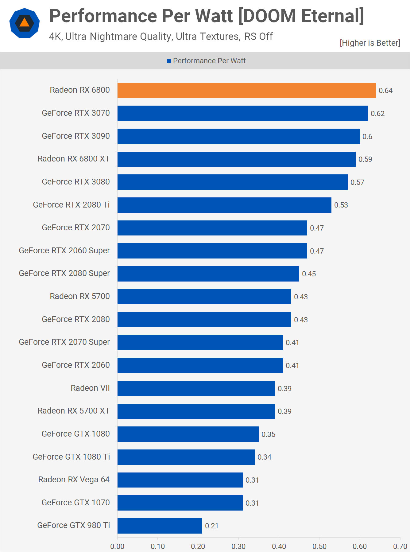
Our operation-per-watt examination of Ampere and RDNA 2 cards showed that both vendors have made significant improvements in this area, just AMD and TSMC have achieved something quite remarkable -- compare the departure between the Radeon RX 6800 and the Radeon 7 in the chart above.
The latter was their first GPU collaboration using the N7 node and in the infinite of less than two years, they've increased the performance-per-watt by 64%. It does beg the question as to how much better the Ampere GA102 could accept been, had Nvidia stayed with TSMC for their production duties.
Managing a GPU factory
How everything is organized inside the fries
When it comes to the processing of instructions and managing data transfers, both Ampere and RDNA 2 follow a similar pattern to how everything is organized inside the chips. Game developers code their titles using a graphics API, to make all of the images; it might exist Direct3D, OpenGL, or Vulkan. These are essentially software libraries, packed full of 'books' of rules, structures, and simplified instructions.
The drivers that AMD and Nvidia create for their chips essentially piece of work as translators: converting the routines issued via the API into a sequence of operations that the GPUs tin can sympathize. After that, it'southward entirely down to the hardware to manage things, with regards to what instructions get done get-go, what role of the chip does them, and then on.
This initial stage of pedagogy management is handled past a collection of units, reasonably centralized in the scrap. In RDNA 2, graphics and compute shaders are routed through separate pipelines, that schedule and dispatch the instructions to the residuum of the chip; the onetime is called the Graphics Control Processor, the latter are Asynchronous Compute Engines (ACEs, for short).

Nvidia only uses one proper noun to describe their prepare of direction units, the GigaThread Engine, and in Ampere it does the same task equally with RDNA 2, although Nvidia doesn't say too much near how it actually manages things. Altogether, these command processors office rather similar a product manager of a factory.
GPUs get their performance from doing everything in parallel, so the adjacent level of system is duplicated beyond the flake. Sticking with the manufacturing plant analogy, these would be akin to a business organization that has a cardinal office, just multiple locations for the manufacturing of goods.
AMD uses the label Shader Engine (SE), whereas Nvidia calls theirs Graphics Processing Clusters (GPC) -- different names, same role.

The reason for this partitioning of the bit is uncomplicated: the control processing units merely can't handle everything, as it would end up being far besides large and complex. Then it makes sense to push some of the scheduling and organization duties further downwardly the line. It besides means each separation segmentation can be doing something completely independent of the others -- so one could be treatment a raft of graphics shaders, while the others are grinding through long, complex compute shaders.
In the case of RDNA 2, each SE contains its ain set of fixed function units: circuits that are designed to do one specific task, that typically tin't be heavily adapted by a programmer.
- Archaic Setup unit of measurement -- gets vertices ready for processing, also as generating more (tessellation) and culling them
- Rasterizer -- converts the 3D earth of triangles into a 2D grid of pixels
- Render Outputs (ROPs) -- reads, writes, and blends pixels
The primitive setup unit runs at a rate of 1 triangle per clock wheel. This might not sound like very much but don't forget that these chips are running at anywhere between 1.8 and 2.2 GHz, and then archaic setup shouldn't always be a bottleneck for the GPU. For Ampere, the primitive unit is establish in the next tier of organisation, and nosotros'll cover that shortly.
Neither AMD nor Nvidia say likewise much about their rasterizers. The latter calls them Raster Engines, we know that they handle 1 triangle per clock wheel, and spit out a number of pixels, only at that place's no farther information to paw, such as their sub-pixel precision, for example.
Each SE in the Navi 21 chip sports 4 banks of eight ROPs, resulting in a total of 128 return output units; Nvidia'southward GA102 packs 2 banks of eight ROPs per GPC, so the full chip sports 112 units. This might seem that AMD has the advantage hither, because more ROPs ways more pixels can be processed per clock. But such units need expert admission to cache and local memory, and we'll say more about that later in this article. For at present, allow's keep looking at how the SE/GPC partitions are further divided.

AMD's Shader Engines are sub-partitioned in what they term Dual Compute Units (DCUs), with the Navi 21 chip fielding x DCUs per SE -- note that in some documents, they're also classed as Workgroup Processors (WGP). In the case of Ampere and the GA102, they're called Texture Processing Clusters (TPCs), with each GPU containing half dozen TPCs. Every cluster in Nvidia'southward design houses something chosen a Polymorph Engine -- essentially, Ampere'south primitive setup units.
They as well run at a charge per unit of one triangle per clock, and although Nvidia'southward GPUs are clocked lower than AMD'due south, they take a lot more TPCs than Navi 21 has SEs. So for the aforementioned clock speed, the GA102 should have a notable reward as the consummate fleck holds 42 primitive setup units, whereas AMD's new RDNA 2 has just iv. But since there are vi TPCs per Raster Engine, the GA102 effectively has vii complete archaic systems, to the Navi 21's 4. Since the latter isn't clocked 75% higher than the one-time, information technology would seem that Nvidia takes a clear lead here, when it comes to geometry handling (though no game is probable to exist express in this area).
The final tier of the chips' organization are the Compute Units (CUs) in RDNA 2 and the Streaming Multiprocessors (SMs) in Ampere -- the production lines of our GPU factories.

These are very much the meat-and-vegetables in the GPU pie, as these concur all of the highly programmable units used to process graphics, compute, and at present ray tracing shaders. Equally you can see in the in a higher place image, each ane takes up a very small-scale portion of the overall die space, but they are nevertheless extremely complex and highly of import to the overall performance of the chip.
Up to now, there hasn't been whatever serious bargain-breakers, when it comes to how everything is laid out and organized in the two GPUs -- the nomenclature is all dissimilar, but their functions are much the same. And because so much of what they do is express by programmability and flexibility, whatsoever advantages one has over the other, just comes down to a sense of scale, i.e. which one has the nigh of that particular thing.
But with the CUs and SMs, AMD and Nvidia take dissimilar approaches to how they get well-nigh processing shaders. In some areas, they share a lot in mutual, simply in that location are plenty of others where that'south not the example.
Counting cores the Nvidia way
Since Ampere ventured into the wild before RDNA 2, we'll take a look at Nvidia's SMs first. There's no point in looking at images of the dice itself now, every bit they tin't tell united states exactly what's inside them, so let'south utilise an organization diagram. These aren't supposed to be representations of how the various components are physically arranged in the bit, only how many of each blazon are present.
Where Turing was a substantial change to its desktop predecessor Pascal (losing a stack of FP64 units and registers, but gaining tensor cores and ray tracing), Ampere is actually a fairly mild update -- on face value, at to the lowest degree. As far as Nvidia's marketing division was concerned, though, the new design more doubled the number of CUDA cores in each SM.

In Turing, the Streaming Multiprocessors contain four partitions (sometimes chosen processing blocks), where each house 16x INT32 and 16x FP32 logic units. These circuits are designed to carry out very specific mathematical operations on 32-flake data values: the INT units handled integers, and the FP units worked on floating point, i.east. decimal, numbers.
Nvidia states that an Ampere SM has a total of 128 CUDA cores, only strictly speaking, this isn't true -- or if we must stick to this count, and so so too did Turing. The INT32 units in that chip could actually handle float values, just just in a very small number of unproblematic operations. For Ampere, Nvidia has opened the range of floating indicate math operations they support to match the other FP32 units. That ways the total number of CUDA cores per SM hasn't really changed; it's only that one-half of them now have more capability.
All of the cores in each SM partition processes the same instruction at any ane time, but since the INT/FP units tin operate independently, the Ampere SM tin handle up to 128x FP32 calculations per cycle or 64x FP32 and 64x INT32 operations together. In Turing, it was just the latter.
So the new GPU has, potentially, double the FP32 output than its predecessor. For compute workloads, especially in professional applications, this is a large stride forward; just for games, the benefits will exist far more muted. This was evident when nosotros beginning tested the GeForce RTX 3080, which uses a GA102 flake with 68 SMs enabled.

Despite having a peak FP32 throughput 121% over the GeForce 2080 Ti, it only averages a 31% increment in frame rates. So why is all that compute ability going to waste? The uncomplicated respond is that it's not, but games aren't running FP32 instructions all the fourth dimension.
When Nvidia released Turing in 2022, they pointed out that on average almost a 36% of the instructions processed by a GPU involved INT32 routines. These calculations are typically run for working out memory addresses, comparisons between two values, and logic flow/control.

And so for those operations, the dual rate FP32 feature doesn't come into play, as the units with the two data pathways can only practice integer or floating bespeak. And an SM partition will only switch to this mode if all 32 threads, being handled by it at the time, have the aforementioned FP32 operation lined upwards to be processed. In all other cases, the partitions in Ampere operate just as they do in Turing.
This means the likes of the GeForce RTX 3080 only has a xi% FP32 advantage over the 2080 Ti, when operating in INT+FP mode. This is why the actual functioning increase seen in games isn't as high as the raw figures propose it should exist.
Other improvements? At that place are fewer Tensor Cores per SM partition, but each one is a lot more capable than those in Turing. These circuits perform a very specific calculations (such every bit multiply 2 FP16 values and accrue the reply with some other FP16 number), and each core at present does 32 of these operations per cycle.

They too support a new feature called Fine-Grained Structured Sparsity and without going into the details of it all, essentially it means the math rate can exist doubled, past pruning out data that doesn't bear upon the reply. Again, this is skillful news for professionals working with neural networks and AI, merely at the moment, in that location's no pregnant benefit for game developers.
The ray tracing cores accept also been tweaked: they can now work independently of the CUDA cores, so while they're doing BVH traversal or ray-primitive intersection math, the rest of the SM tin still be processing shaders. The part of the RT Core that handles the testing of whether or not a ray intersects a primitive has doubled in performance, too.
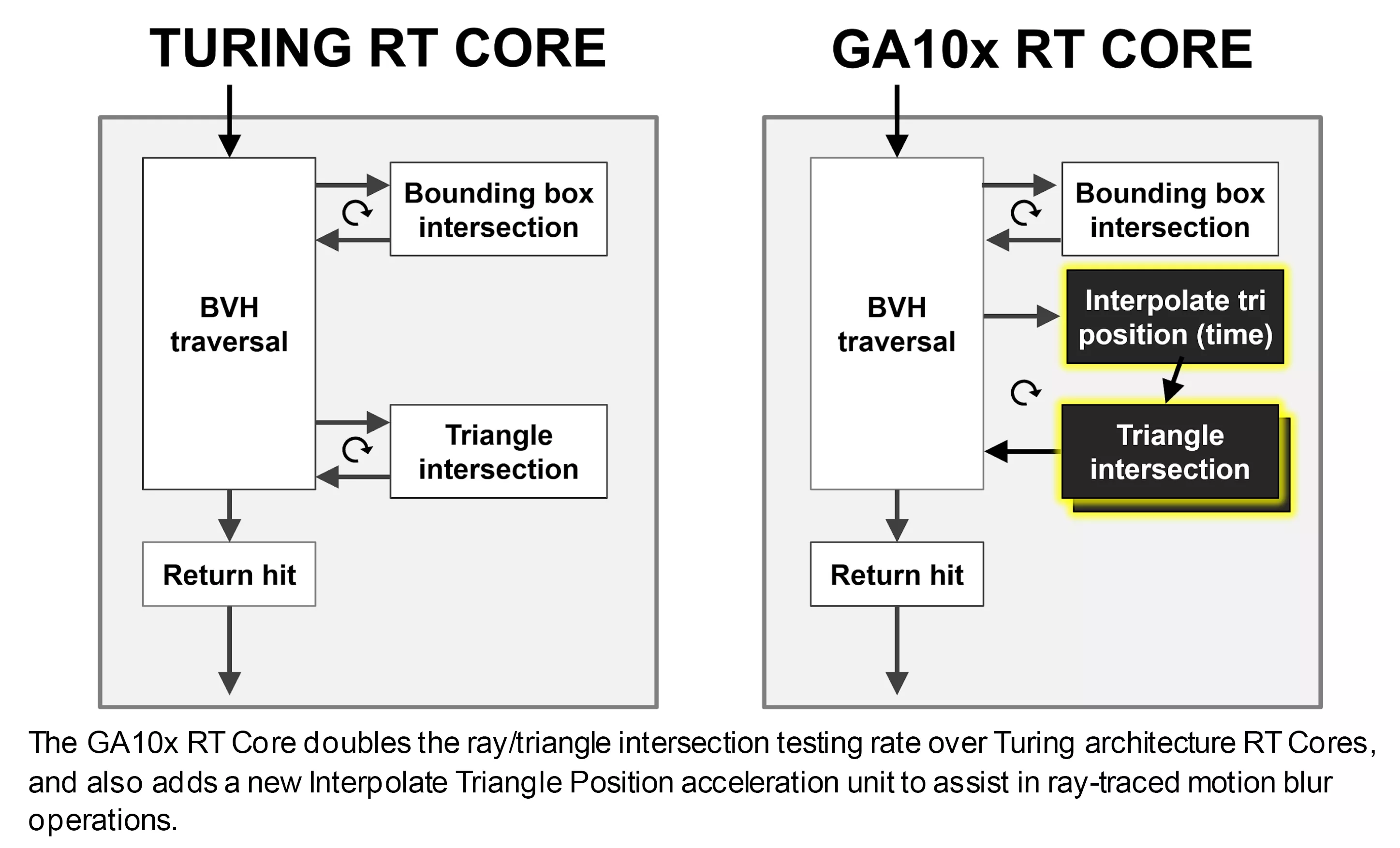
The RT Cores too sport additional hardware to help employ ray tracing to motion blur, just this feature is currently but exposed through Nvidia's proprietary Optix API.
There are other tweaks, but the overall arroyo has been i of sensible merely steady development, rather than a major new blueprint. But given that at that place was nothing particularly incorrect with Turing'south raw capabilities in the first identify, information technology's not surprising to see this.
So what about AMD -- what have they washed to the Compute Units in RDNA 2?
Tracing the rays fantastic
On face value, AMD haven't changed much about the Compute Units -- they still comprise ii sets of an SIMD32 vector unit of measurement, an SISD scalar unit, textures units, and a stack of various caches. There's been some changes regarding what information types and associated math operations they can practice, and nosotros'll say more near those in a moment. The most notable change for the general consumer is that AMD at present offer hardware acceleration for specific routines within ray tracing.
This part of the CU performs ray-box or ray-triangle intersection checks -- the same as the RT Cores in Ampere. Notwithstanding, the latter also accelerates BVH traversal algorithms, whereas in RDNA 2 this is done via compute shaders using the SIMD 32 units.

No thing how many shader cores one has or how loftier their clock rates are, going with customized circuits that are designed to do just one job is always going to be ameliorate than a generalized approach. This is why GPUs were invented in the first place: everything in the world of rendering can be washed using a CPU, merely their general nature makes them unsuitable for this.
The RA units are side by side to the texture processors, because they're really role of the same structure. Back in July 2022, we reported on the appearance of a patent filed by AMD which detailed using a 'hybrid' approach to handling the key algorithms in ray tracing...
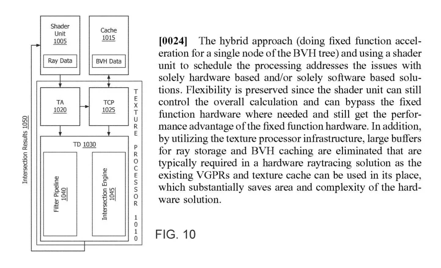
While this system does offering greater flexibility and removes the need to have portions of the die doing nix when there'south ray tracing workload, AMD'southward starting time implementation of this does have some drawbacks. The near notable of which is that the texture processors can but handle operations involving textures or ray-archaic intersections at whatever i time.
Given that Nvidia'due south RT Cores now operate fully independently of the remainder of the SM, this would seem to give Ampere a singled-out pb, compared to RNDA 2, when it comes to grinding through the dispatch structures and intersection tests required in ray tracing.
Although nosotros've but briefly examined the ray tracing performance in AMD'southward latest graphics cards, so far nosotros did find that the bear on of the use of ray tracing was very dependent on the game being played.
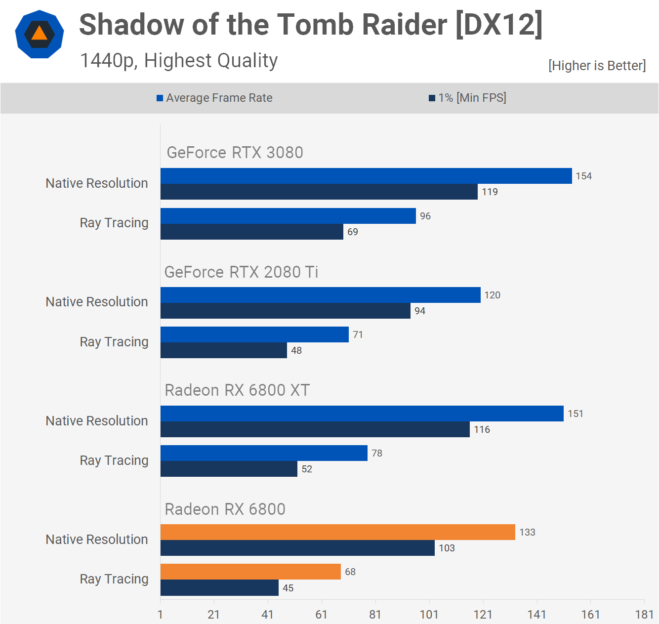
In Gears v, for case, the Radeon RX 6800 (which uses a 60 CU variant of the Navi 21 GPU) only took a 17% frame charge per unit striking, whereas in Shadow of the Tomb Raider, this rose to an average loss of 52%. In comparison, Nvidia's RTX 3080 (using a 68 SM GA102) saw average frame rate losses of 23% and 40% respectively, in the two games.
A more detailed analysis of ray tracing is needed to say annihilation more about AMD's implementation, but as a kickoff iteration of the engineering, information technology does appear to be competitive but sensitive to what application is doing the ray tracing.
As previously mentioned, the Compute Units in RDNA ii now support more data types; the nearly notable inclusions are the low precision information types such as INT4 and INT8. These are used for tensor operations in motorcar learning algorithms and while AMD take a separate architecture (CDNA) for AI and data centers, this update is for use with DirectML.

This API is a recent improver to Microsoft's DirectX 12 family and the combination of hardware and software will provide better acceleration for denoising in ray tracing and temporal upscaling algorithms. In the case of the latter, Nvidia have their own, of course, chosen DLSS. Their system uses the Tensor Cores in the SM to perform role of the calculations, simply given that a like process can be constructed via DirectML, it might seem that these units are somewhat redundant. Nevertheless, in both Turing and Ampere, the Tensor Cores also handle all math operations involving FP16 information formats.
With RDNA 2, such calculations are done using the shader units, using packed data formats, i.e. each 32-bit vector register holds two 16-bit ones. So which is the ameliorate approach? AMD labels their SIMD32 units as vector processors, considering they issue one instruction for multiple data values.
Each vector unit contains 32 Stream Processors, and since each ane of these simply works on a single piece of data, the bodily operations themselves are scalar in nature. This is essentially the aforementioned as an SM partition in Ampere, where each processing block also carries ane instruction on 32 data values.
Simply where a entire SM in Nvidia'southward design tin procedure up to 128 FP32 FMA calculations per wheel (fused multiply-add together), a single RDNA 2 Compute Unit only does 64. Using FP16 raises this to 128 FMA per cycle, which is the same as Ampere'due south Tensor Cores when doing standard FP16 math.
Nvidia'due south SMs can process instructions to handle integer and float values at the same time (due east.g. 64 FP32 and 64 INT32), and has contained units for FP16 operations, tensor math, and ray tracing routines. AMD's CUs do the majority of the workload on the SIMD32 units, although they practice accept separate scalar units that support simple integer math.
Then it would seem that Ampere has the edge hither: the GA102 has more SMs than Navi 21 has CUs, and they're packing a bigger punch, when it comes to peak throughput, flexibility, and features on offer. But AMD has a rather nice trick card upwards their sleeve.
Feeding those hungry hungry hippos
Retentiveness system, multi-level caches
Having a GPU with thousands of logic units, all blazing their way through fancy math, is all well and good -- but they'd be floundering at sea if they couldn't exist fed apace plenty, with the instructions and data they require. Both designs sport a wealth of multi-level caches, boasting huge amounts of bandwidth.
Let's take a look at Ampere'due south beginning. Overall there have been some notable changes internally. The amount of Level 2 cache has increased by fifty% (the Turing TU102 sported 4096 kB respectively), and the Level 1 caches in each SM accept both doubled in size.

As before, Ampere's L1 caches are configurable, in terms of how much cache space can be allocated for information, textures, or general compute use. However, for graphics shaders (e.g. vertex, pixel) and asynchronous compute, the cache is actually set to:
- 64 kB for information and textures
- 48 kB for shared general retentiveness
- 16 kB reserved for specific operations
Merely when running in full compute mode, does the L1 go fully configurable. On the plus side, the amount of bandwidth bachelor has besides doubled, as the cache can now read/write 128 bytes per clock (although at that place'southward no word on whether or not the latency has been improved, besides).
The residual of the internal retentivity system has remained the aforementioned in Ampere, simply when nosotros move just outside the GPU, at that place'south a nice surprise in store for us. Nvidia partnered with Micron, a DRAM manufacturer, to use a modified version of GDDR6 for their local retentivity needs. This is still essentially GDDR6 but the data bus has been entirely replaced. Rather than using a conventional 1 bit per pin ready, where the signal just bounces very rapidly between two voltages (aka PAM), GDDR6X uses four voltages:

With this modify, GDDR6X effectively transfers two bits of data per pivot, per wheel -- so for the same clock speed and pin count, the bandwidth is doubled. The GeForce RTX 3090 sports 24 GDDR6X modules, running in single aqueduct mode and rated to 19 Gbps, giving a peak transfer bandwidth of 936 GB/southward.
That's an increase of 52% over the GeForce RTX 2080 Ti and non something to exist dismissed lightly. Such bandwidth figures have only been accomplished in the past by using the likes of HBM2, which can be costly to implement, when compared to GDDR6.
However, merely Micron makes this memory and the use of PAM4 adds additional complexity to the product process, requiring far tighter tolerances with the signalling. AMD went downwards a different route -- instead of turning to an outside agency for help, they used their CPU division to bring something new to the table. The overall memory organisation in RDNA 2 hasn't inverse much compared to its predecessor -- there are only two major changes.

Each Shader Engine now has 2 sets of Level 1 caches, but as they are at present sporting 2 banks of Dual Compute Units (RDNA only had the one), this alteration is to be expected. But shoehorning 128 MB of Level 3 cache into the GPU? That surprised a lot of people. Utilizing the SRAM design for the L3 cache establish in their EPYC-range of Zen two server chips, AMD have embedded two sets of 64 MB loftier-density cache into the chip. Information transactions are handled past 16 sets of interfaces, each shifting 64 bytes per clock wheel.
The so-called Infinity Cache has its own clock domain, and can run at up ane.94 GHz, giving a peak internal transfer bandwidth of 1986.vi GB/s. And because it'south non external DRAM, the latencies involved are exceptionally low. Such cache is perfect for storing ray tracing acceleration structures and since BVH traversal involves a lot of data checking, the Infinity Cache should notably assistance with this.

At the moment, it's non articulate if the Level three cache in RDNA ii operates in the aforementioned fashion every bit in a Zen 2 CPU: i.eastward. equally a Level ii victim cache. Ordinarily, when the last level of cache needs to be cleared to make room for new data, any new requests for that information will have to get to the DRAM.
A victim cache stores data that'southward been flagged for removal from the adjacent tier of retentiveness, and with 128 MB of it to manus, the Infinity Cache could potentially shop 32 complete sets of L2 cache. This system results in less demand being placed on the GDDR6 controllers and DRAM.
Older GPU designs by AMD have struggled with a lack of internal bandwidth, particularly equally one time their clock speeds were ramped upward, but the extra enshroud will become a long manner to making this upshot fade into the groundwork.

And so which pattern is improve here? The use of GDDR6X gives the GA102 enormous bandwidth to the local retentivity, and the larger caches will help reduce the bear upon of cache misses (which stall the processing of a thread). Navi 21's massive Level 3 cache means the DRAM doesn't have to tapped every bit often, and leverages the ability to run the GPU at higher clock speeds without information starvation.
AMD's decision to stick with GDDR6 means at that place are more sources of memory available for third party vendors, meanwhile any company making a GeForce RTX 3080 or 3090 will have to utilize Micron. And while GDDR6 comes in a variety of modules densities, GDDR6X is currently limited to 8 Gb.
The cache organization inside RDNA 2 is arguably a better approach than that used in Ampere, equally using multiple levels of on-die SRAM will always provide lower latencies, and improve functioning for a given power envelope, than external DRAM, regardless of the latter'southward bandwidth.
The ins and outs of a GPU
Rendering pipelines
Both architectures characteristic a raft of updates to the front and back ends of their rendering pipelines. Ampere and RDNA 2 fully sport mesh shaders and variable rate shaders in DirectX12 Ultimate, although Nvidia'south scrap does have more geometry functioning thanks to its greater number of processors for these tasks.
While the use of mesh shaders will enable developers to create e'er more realistic environments, no game is ever going to take its operation be entirely leap to this stage in the rendering process. This is because the bulk of the hardest piece of work is at the pixel or ray tracing stages.

This is where the utilise of variable charge per unit shaders come into play -- basically, the procedure involves use shaders for lighting and colour on a block of pixels, rather than private ones. It's akin to decreasing the resolution of the game in order to better operation, but since it can exist applied to just selected regions, the loss in visual quality isn't readily apparent.
Simply both architectures have likewise been given an update to their render output units (ROPs), every bit this will improve operation at high resolutions, whether or not variable rate shaders are used. In all previous generations of their GPUs, Nvidia tied the ROPs to the retentivity controllers and Level ii cache.
In Turing, eight ROP units (collectively called a partition) were direct linked to one controller and a 512 kB slice of the enshroud. Adding more ROPs creates a problem, as it requires more than controllers and cache, so for Ampere, the ROPs are now entirely allocated to a GPC. The GA102 sports 12 ROPs per GPC (each i processing 1 pixel per clock cycle), giving a full of 112 units for the full chip.
AMD follows a similar system to Nvidia'south former approach (i.e. tied to a memory controller and L2 enshroud piece), although their ROPs are primarily use the Level one cache for pixel read/writes and blending. In the Navi 21 chip, they've been given a much needed update and each ROP division now handles 8 pixels per bicycle in 32-bit color, and four pixels in 64-bit.
Something else that Nvidia have brought to the tabular array with Ampere is RTX IO -- a data handling system that allows the GPU to directly access the storage bulldoze, copy across the data information technology needs, and and so decompress it using the CUDA cores. At the moment, though, the organization can't be used in whatsoever game, considering Nvidia are using the DirectStorage API (another DirectX12 enhancement) to control information technology and that's not set up for public release yet.

The methods used at the moment involve having the CPU manage all this: it receives the data asking from the GPU drivers, copies the data from the storage drive to the organisation memory, decompresses it, and then copies it beyond to the graphics card's DRAM.
Besides the fact that this involves a lot of wasted copying, the mechanism is serial in nature -- the CPU processes 1 request at a time. Nvidia are challenge figures such as "100x data throughput" and "20x lower CPU utilization," simply until the system can exist tested in the existent earth, such figures can't exist examined further.

When AMD introduced RDNA 2 and the new Radeon RX 6000 graphics cards, they launched something called Smart Access Memory. This is not their reply to Nvidia's RTX IO -- in fact, it'southward not even really a new characteristic. By default, the PCI Express controller in the CPU can address up to 256 MB of the graphics card's retentivity, per private access request.
This value is set by the size of the base accost register (BAR) and every bit far back equally 2008, there has been an optional feature in the PCI Express 2.0 specification to permit information technology exist resized. The benefit of this is that fewer admission requests have to be processed in order to accost the whole of the card's DRAM.
The office requires support by the operating system, CPU, motherboard, GPU, and its drivers. At present, on Windows PCs, the system is limited to a specific combination of Ryzen 5000 CPUs, 500 series motherboards, and Radeon RX 6000 graphics cards.
This simple feature gave some startling results when we tested it -- performance boosts of fifteen% at 4K are not to be dismissed lightly, then information technology should come up every bit no surprise that Nvidia have said that they'll be offering the characteristic for the RTX 3000 range at some point in the near future.
Whether or not resizable BAR support is rolled out for other platform combinations remains to be seen, but its use is certainly welcome, even though it'due south not an architectural characteristic of Ampere/RDNA 2 as such.
Multimedia engine, video output
The GPU earth is normally dominated past cadre count, TFLOPS, GB/south, and other headline-grabbing metrics, but thank you to the rise of YouTube content creators and live gaming streams, the display and multimedia engine capabilities are also of considerable note.
The demand for ultra high refresh rates, at all resolutions, has grown as the price of monitors supporting such features has dropped. Two years ago, a 144 Hz 4K 27" HDR monitor would have set you back $ii,000; today, you tin can get something similar for almost one-half the price.
Both architectures provide a display output via HDMI two.1 and DisplayPort 1.4a. The quondam offers more signal bandwidth, but they're both rated for 4K at 240 Hz with HDR and 8K at threescore Hz. This is accomplished by using either iv:2:0 chroma subsampling or DSC 1.2a. These are video bespeak compression algorithms, which provide a significant reduction in bandwidth requirements, without too much loss of visual quality. Without them, even HDMI 2.ane's peak bandwidth of 6 GB/due south wouldn't be enough to transmit 4K images at a rate of 6 Hz.

Ampere and RDNA 2 besides support variable refresh rate systems (FreeSync for AMD, Grand-Sync for Nvidia) and when it comes to the encoding and decoding of video signals, there's no discernable difference hither either.
No thing which processor you expect at, y'all'll discover support for 8K AV1, 4K H.264, and 8K H.265 decoding, although exactly how well they both perform in such situations hasn't been thoroughly examined still. Neither company gives much detail about the actual innards of their display and multimedia engines. Equally of import as they are these days, it'southward still the rest of the GPU that garners all of the attending.
Different strokes for different folks
Built for compute, built for gaming
Enthusiasts of GPU history will know that AMD and Nvidia used to take rather dissimilar approaches to their architectural choices and configurations. Simply as 3D graphics accept become increasingly dominated by the compute world and the homogenization of APIs, their overall designs have been increasingly similar.
And rather than the demands of rendering in today's games setting the tone for the architectures, it'southward the market sectors that the GPU industry has expanded into that's steering the direction. At the time of writing, Nvidia has three fries using the Ampere technology: the GA100, GA102, and GA104.

The concluding i is simply a cut-downwardly version of the GA102 -- it simply has fewer TPCs per GPC (and ane less GPU overall) and two thirds the Level 2 cache. Everything else is exactly the same. The GA100, on the other hand, is a dissimilar fauna altogether.
It has no RT Cores and no CUDA cores with INT32+FP32 back up; instead it packs in a raft of additional FP64 units, more load/store systems, and an enormous amount of L1/L2 cache. Information technology also has no display or multimedia engine whatever; this is because it'south designed entirely for large scale compute clusters for AI and information analytics.
The GA102/104, though, need to cover every other marketplace that Nvidia targets: gaming enthusiasts, professional graphics artists and engineers, and pocket-size scale AI and compute work. Ampere needs to be a 'jack of all trades' and a primary of all of them -- no like shooting fish in a barrel task.

RDNA 2 was designed for merely gaming, in PCs and consoles, although information technology could merely equally well plough its hand to the same areas as Ampere sells in. However, AMD chose to go on their GCN architecture going and update it for the demands of today's professional clients.
Where RDNA ii has spawned 'Big Navi', CDNA could be said to have spawned 'Large Vega' - the Instinct MI100 houses their Arcturus chip, a 50 billion transistor GPU that sports 128 Compute Units. And like Nvidia'due south GA100, information technology too contains no brandish nor multimedia engines.
Although Nvidia heavily dominates the professional person market with Quadro and Tesla models, the likes of the Navi 21 simply are not aimed at competing confronting these and has been designed accordingly. Then does that brand RDNA 2 the amend architecture; does the requirement for Ampere to fit into multiple markets constrain it in any style?
When you look at the prove, the answer would announced to be: no.
AMD will be releasing the Radeon RX 6900 XT soon, which uses a complete Navi 21 (no CUs disabled), which may perform too equally the GeForce RTX 3090 or ameliorate. But the GA102 in that card isn't fully enabled either, then Nvidia always take the choice to update that model with a 'Super' version, every bit they did with Turing last twelvemonth.
It could exist argued that because RDNA two is being used in the Xbox Series X/S and PlayStation five, game developers are going to favor that compages volition their game engines. But you lot only take to look at when GCN was used in the Xbox 1 and PlayStation 4 to see how this is probable to play out.
The kickoff release of the former, in 2022, used a GPU built around the GCN ane.0 architecture -- a design that didn't appear in desktop PC graphics cards until the following year. The Xbox One X, released in 2022, used GCN two.0, a mature design was already over iii years old by then.

And so did all games made for the Xbox One or PS4 that got ported over to the PC automatically run better on AMD graphics cards? They did non. So nosotros can't assume that this time will exist different with RDNA 2, despite its impressive feature set.
But none of this ultimately matters, equally both GPU designs are exceptionally capable and marvels of what can be achieved in semiconductor fabrication. Nvidia and AMD bring different tools to the bench, because they're trying to crack dissimilar problems; Ampere aims to exist all things to all people, RDNA ii is more often than not about gaming.
This fourth dimension circular, the battle has fatigued to a stalemate, even though each tin can merits victory in a specific area or ii. The GPU wars will continue throughout next year, and a new combatant volition enter the fray: Intel, with their Xe series of chips. At least nosotros won't have to wait another two years to run across how that fight runs its class!
Shopping Shortcuts:
- Nvidia GeForce RTX 3090 on Amazon
- Nvidia GeForce RTX 3080 on Amazon
- AMD Radeon RX 6800 XT on Amazon
- AMD Radeon RX 6800 on Amazon
- Nvidia GeForce RTX 3070 on Amazon
- Nvidia GeForce RTX 3060 Ti on Amazon

Source: https://www.techspot.com/article/2151-nvidia-ampere-vs-amd-rdna2/
Posted by: riveraferemabight.blogspot.com
0 Response to "Nvidia Ampere vs. AMD RDNA 2: Battle of the Architectures"
Post a Comment